The Xiaomi Mi Power Bank 3 Pro is Xiaomi’s third generation of power bank. This power bank supports two USB-A and one bi-directional USB Type-C fast charging protocols. Let’s begin to dismantle it to see its internal structure.
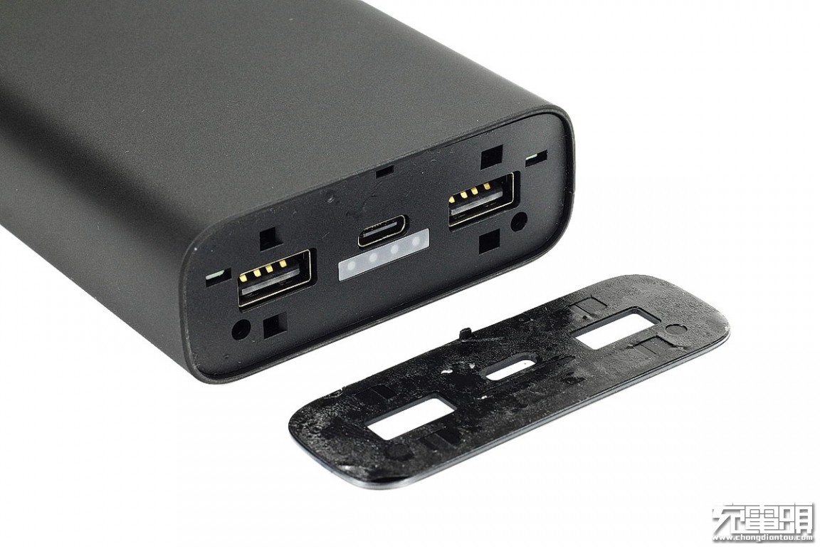
First of all, use an insulated pry to remove the plastic faceplate of the output end. The double-sided tape can be found on the back of the cover.
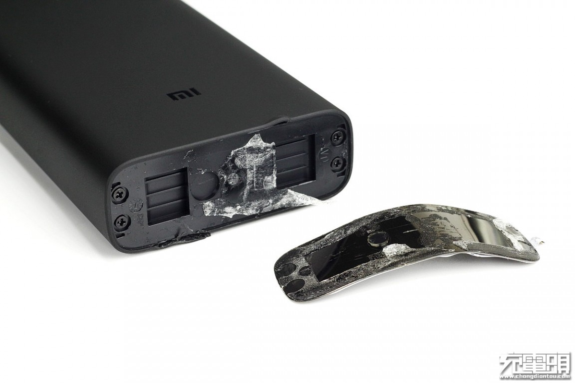
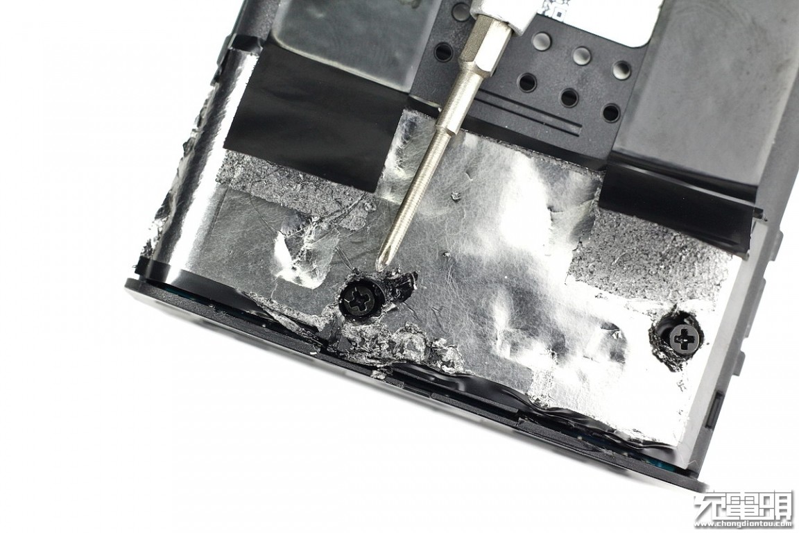
Now take out the blocking plate at the bottom. The plate uses double tape as well. With the plate removed, four screws which secure the blocking plate to the bottom can be seen. Take out the screws.
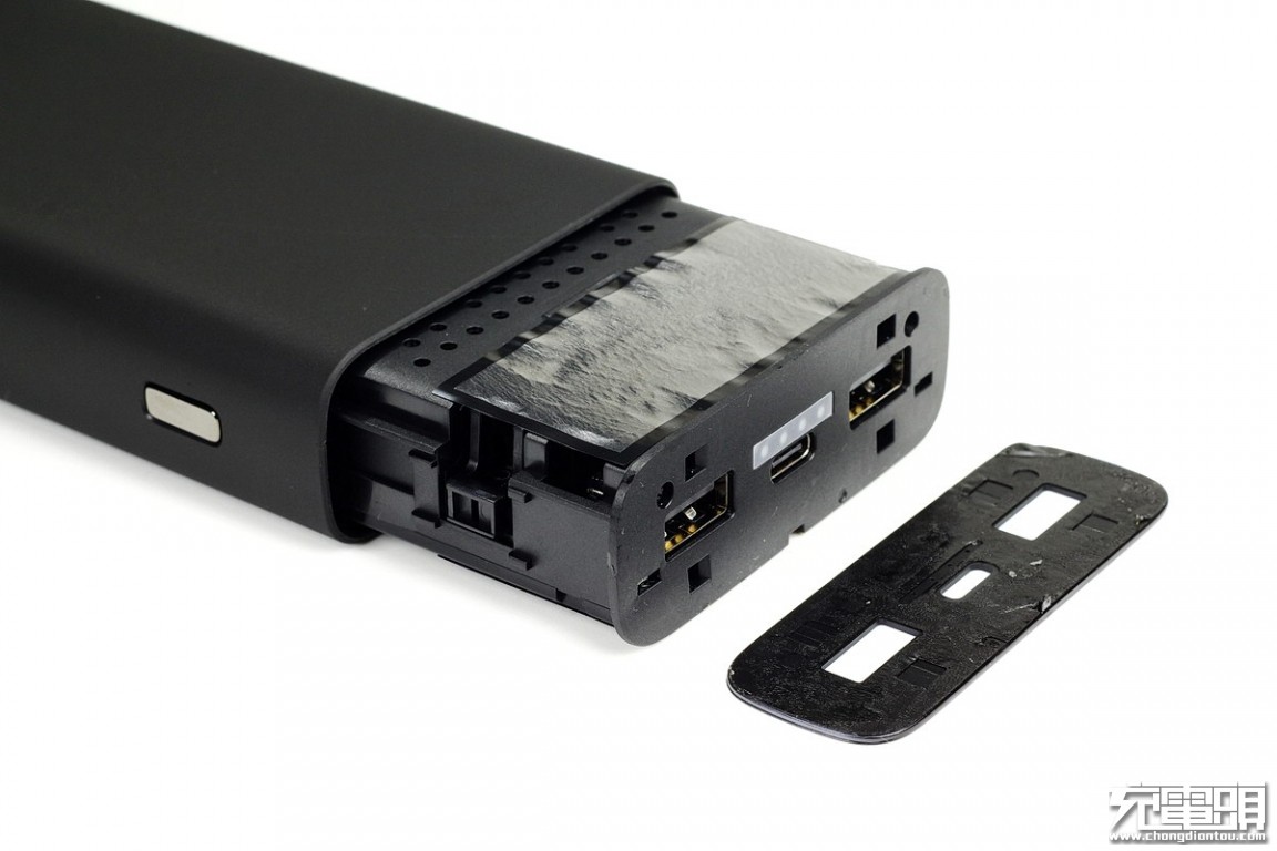
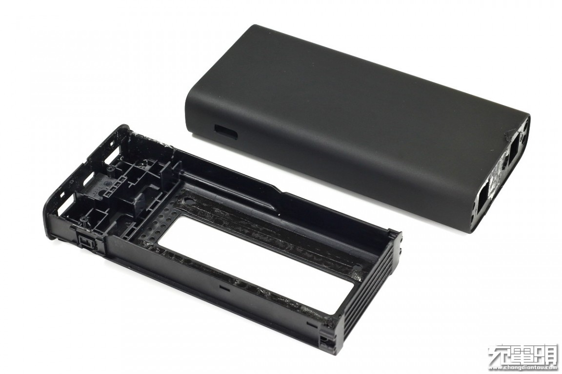
Once the screws are removed, the whole unit can slide out of the channel chassis. At present, most chargers adopt this design. There are four indicators which show battery power.
This is the internal middle frame. A graphite ticker is on the left.
Look at the other side of the middle frame. There are three graphite stickers.
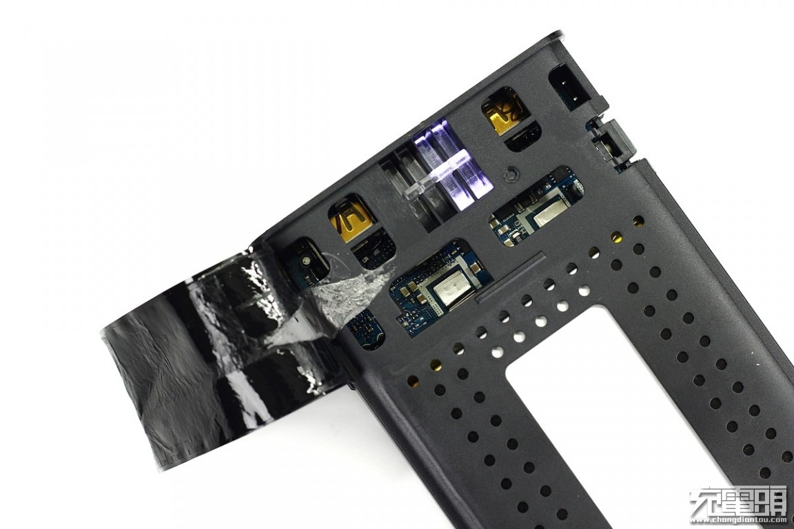
Uncover the sticker, and the PCBA unfolds. The luminous transparent module is universally called a light pipe. This component works with the LED indicator.
Two screws are placed under the graphite sticker.

The internal middle frame is composed of two parts: top faceplate and bottom faceplate.
The middle frame consists of a roller cage. With other small components, this frame is more stable and shock resistant. When deciding the position of PCAB, the designer has taken a circuit layout into consideration.
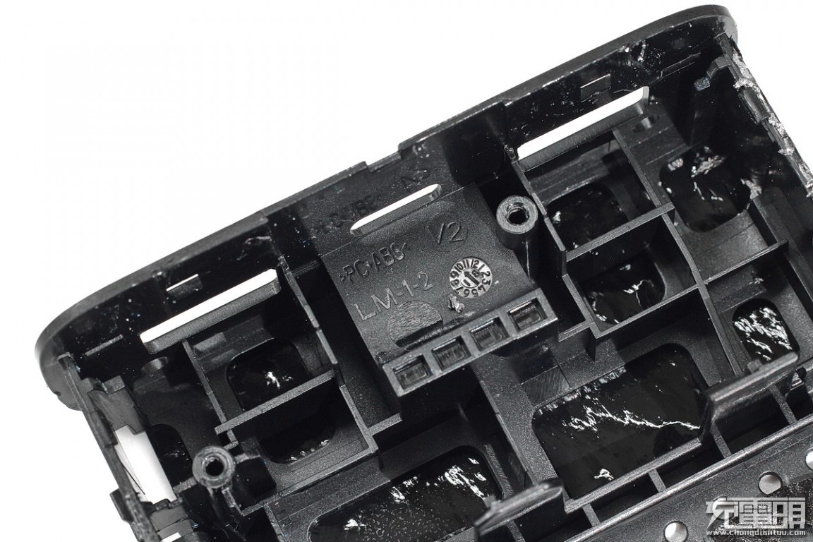
The middle frame is made of PC and ABS.
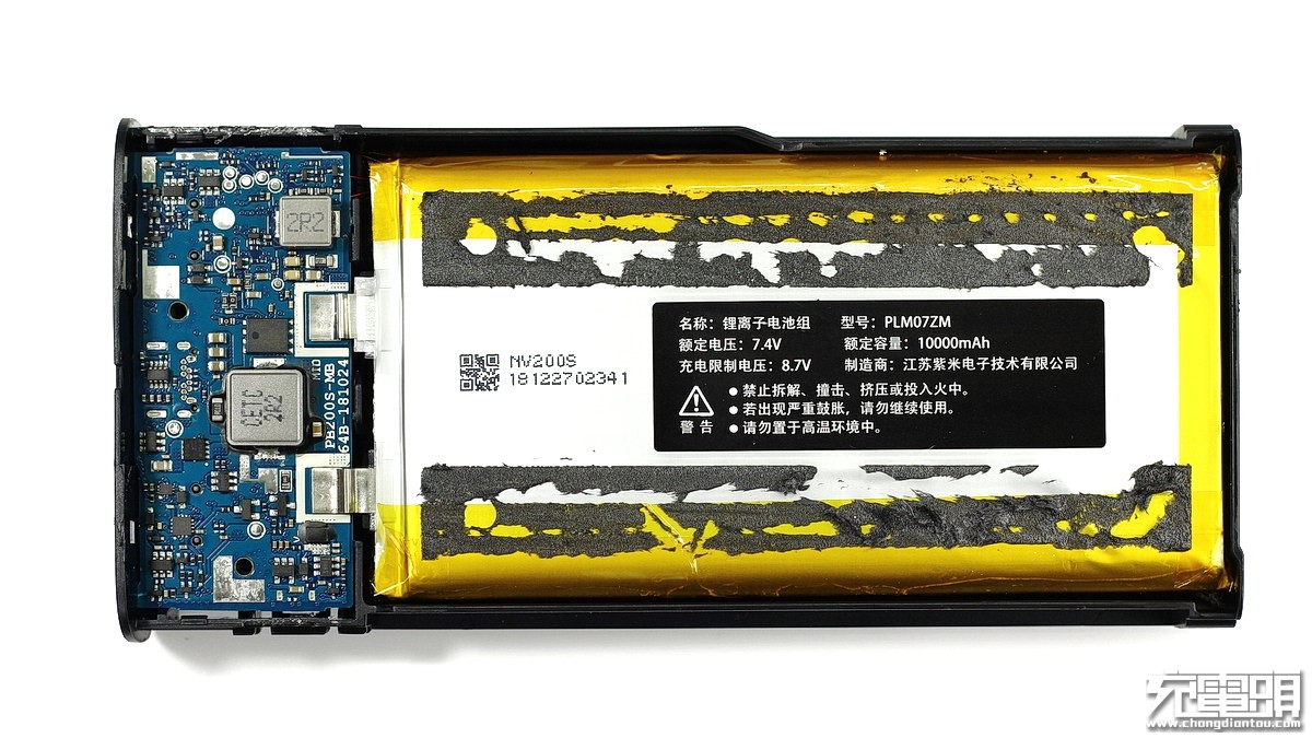
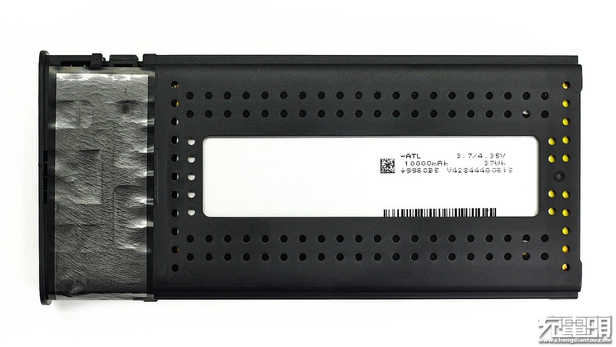
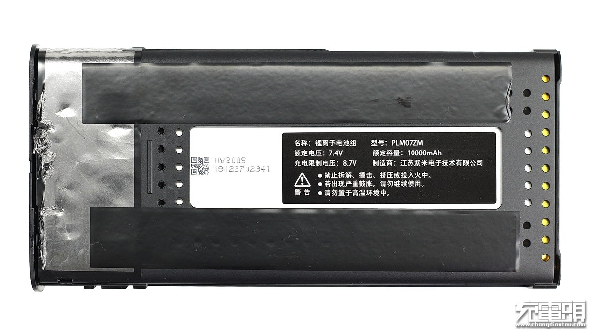
The battery resides in the middle frame by the black sponge tape. These are the specifications of the battery module. Its model number is PLM07ZM; its rated voltage is 7.4V; its limited charging voltage is 8.7V; its manufacturer is ZMI.
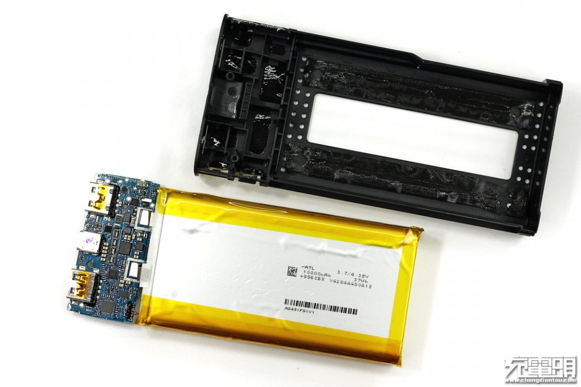
Separate the battery from the middle frame. We can see some information on the other side of the batter.
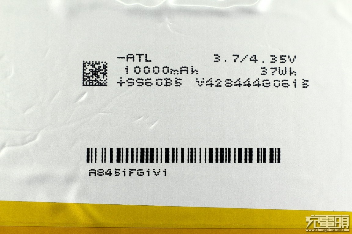
The cell is provided by ATL. The ATL lithium polymer pack is made of two cells in parallel.
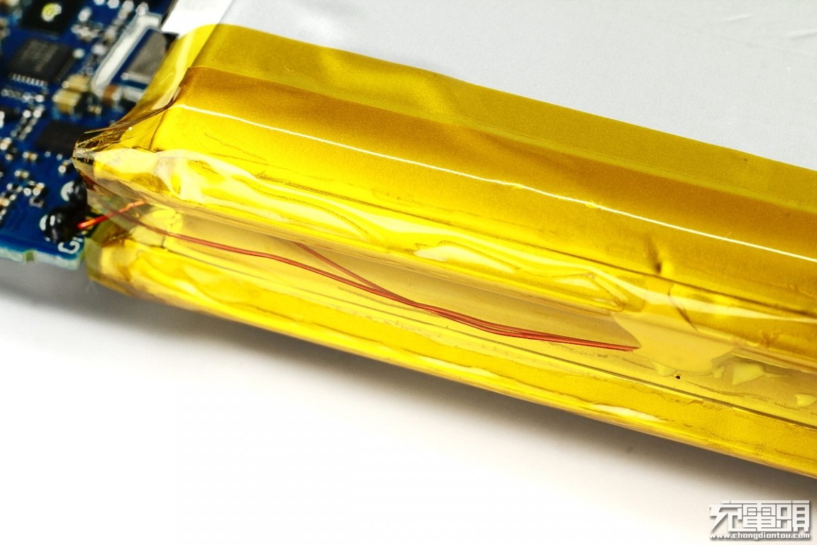
The NTC pack thermistor is provided for thermal protection of the pack.
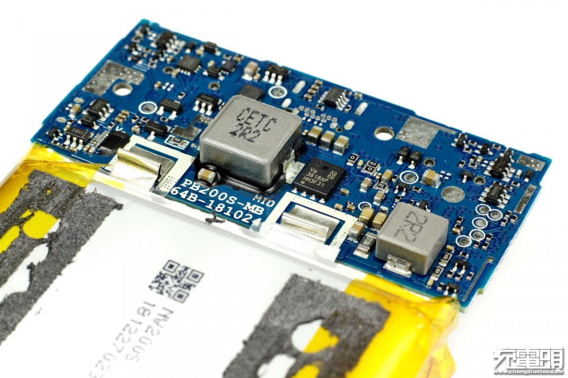
The PCB comes with two electrical inductors.
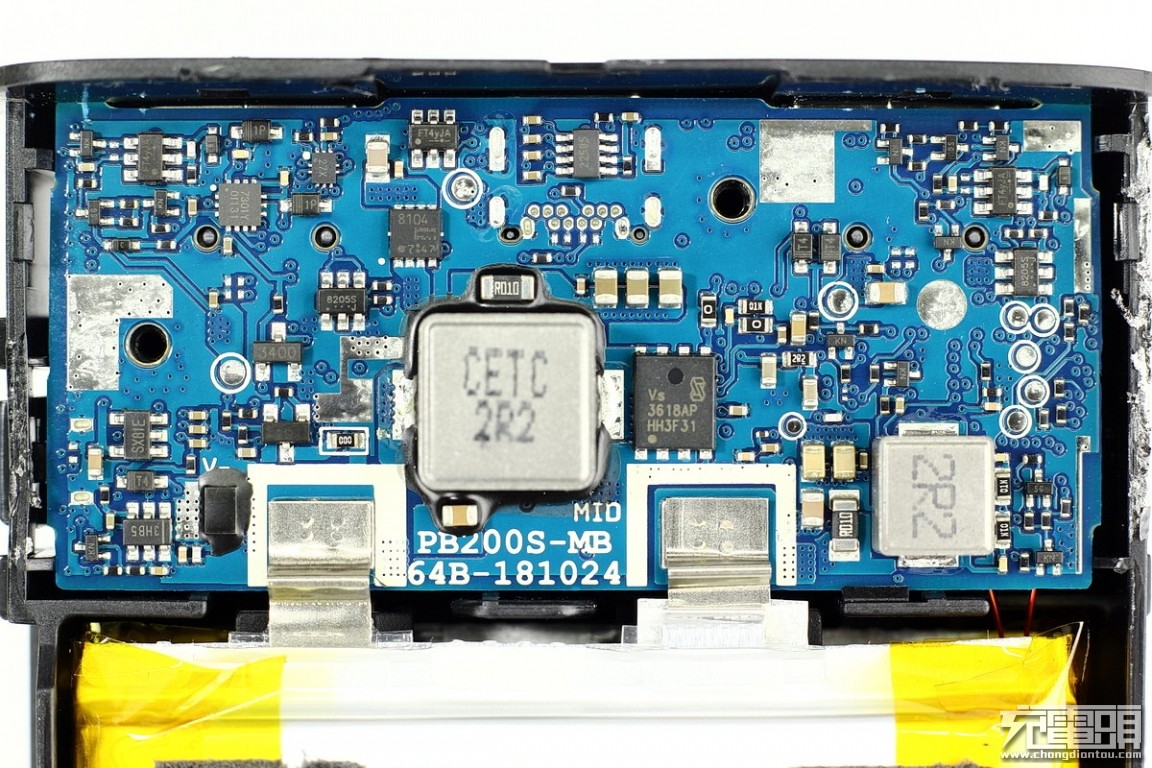
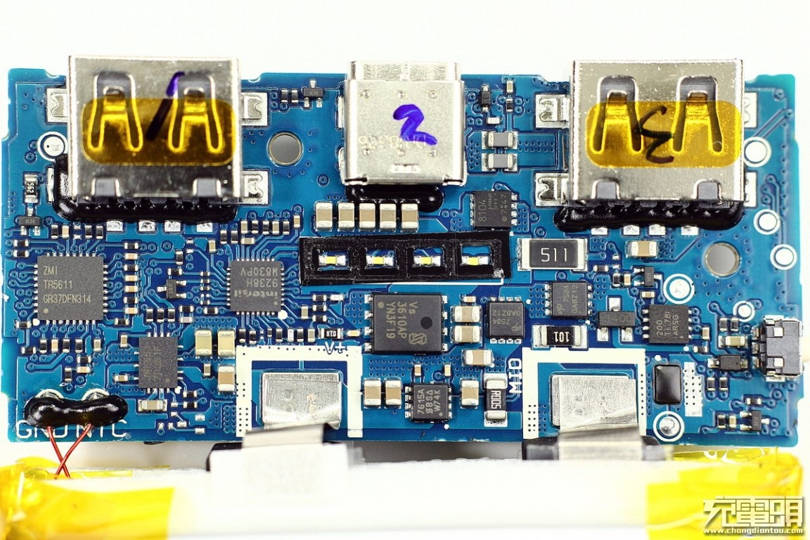
It’s the back of the PCBA. The big inductor is manufactured by CETC.
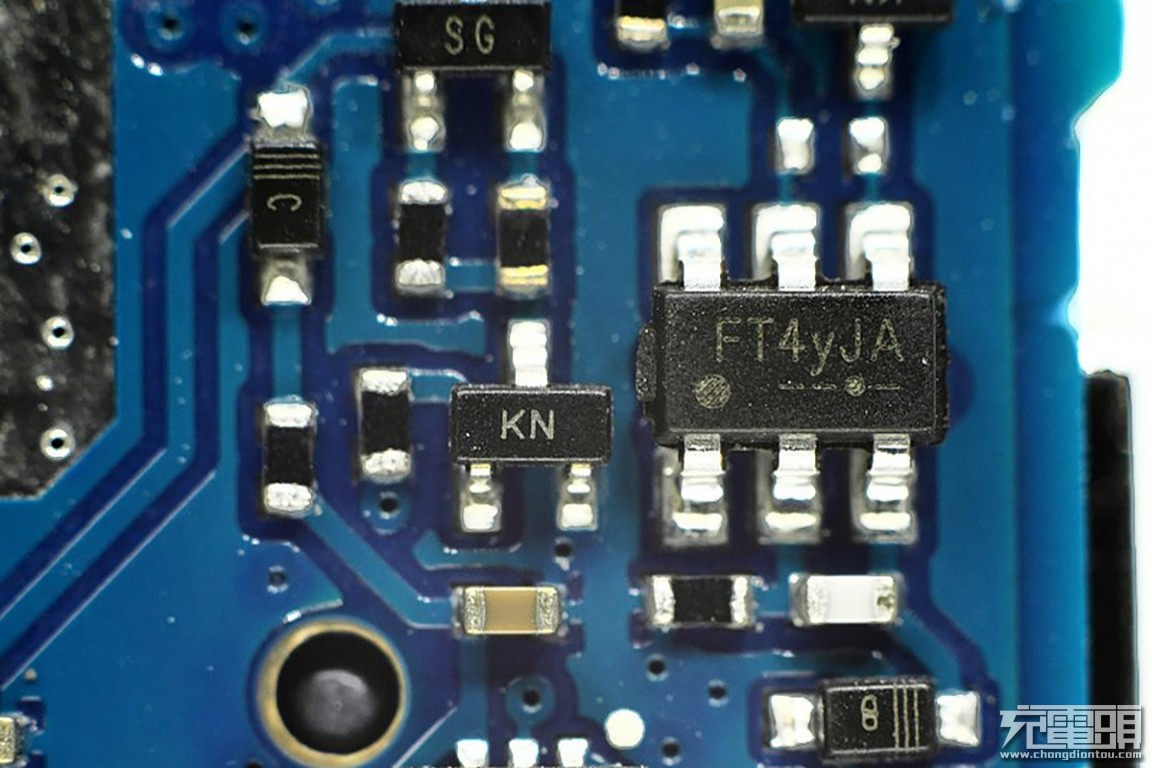
The module labeled as FT4yJA is the Fitipower FP6601Q- a fast charge protocol controller for Hisilicon Fast Charging Protocol(FCP) and Qualcomm Quick Charge 2.0/3.0 USB interface.
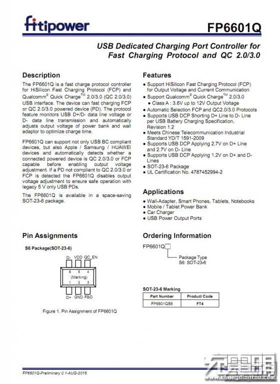
It’s the information on the FP6601Q.
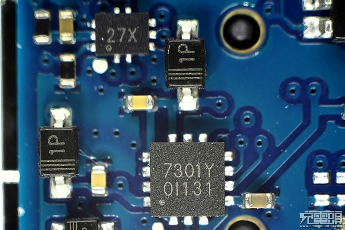
This is the USB-C controller which supports USB PD handshake. The module labeled as 27X is the SGM7227 switch from SG Micro Corporation. It is compatible with high-speed USB 2.0.
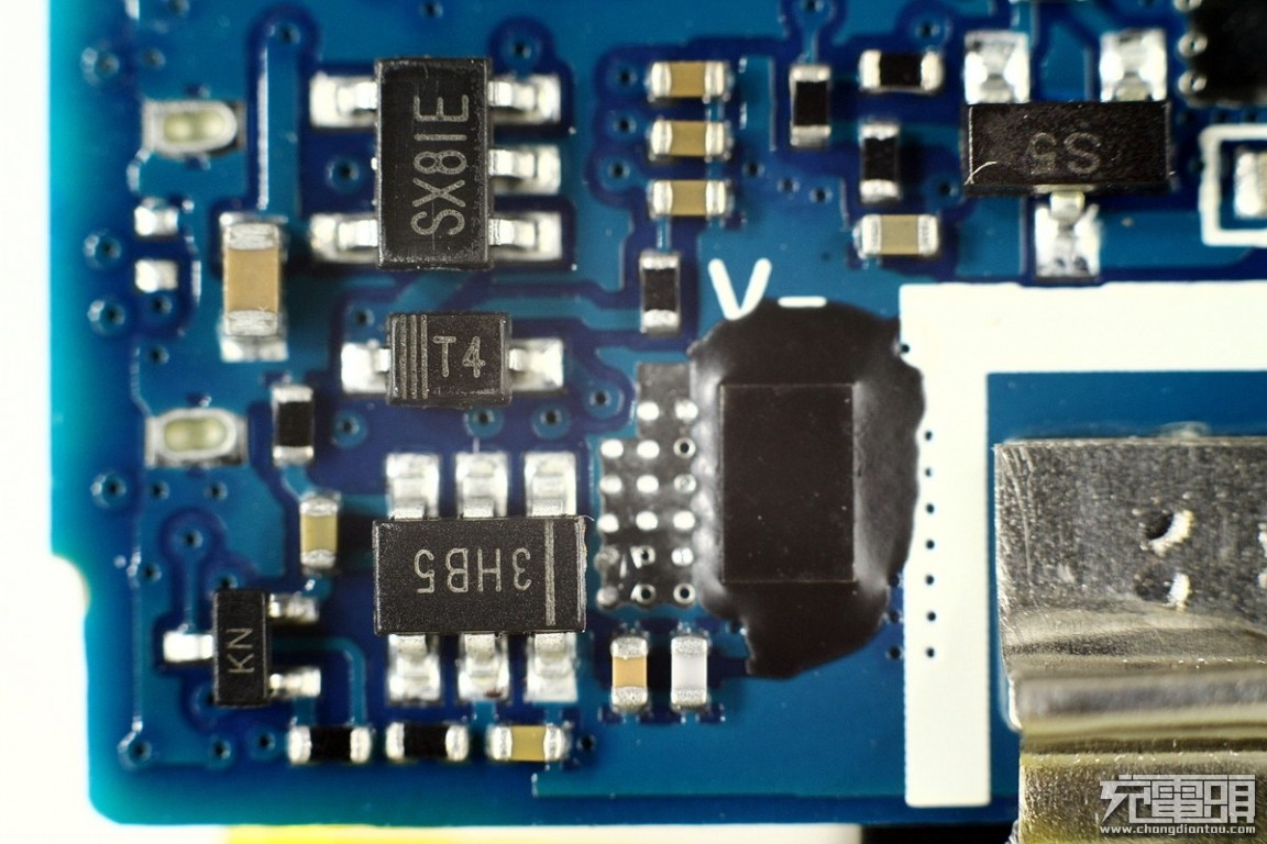
The module labeled as 3HB5 is the battery protection IC.
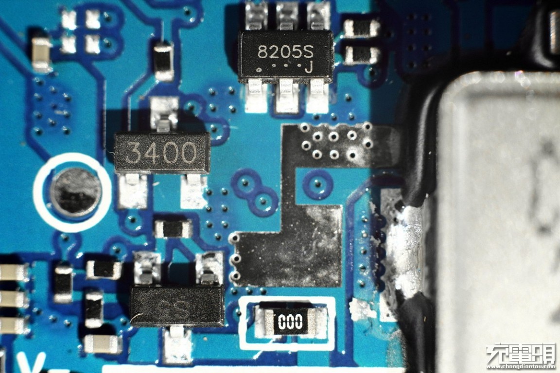
The 8205S is the output switch. Its circuit board adopts multiple processes which are good for its heat dissipation.
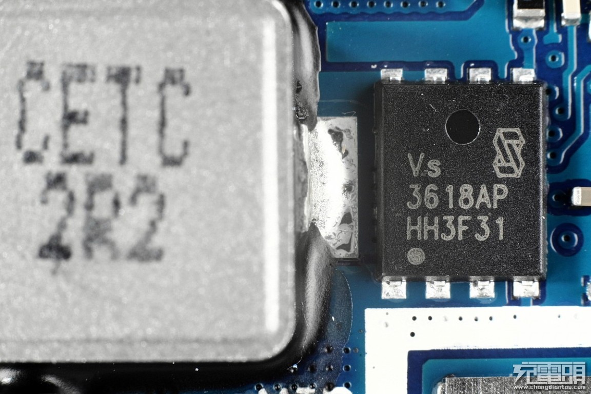
It’s Vanguard’s VS 3618AP switch.
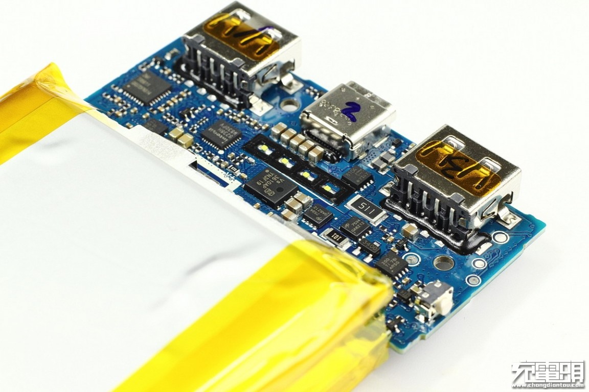
This is the USB-A port.
It’s the front of the PCBA.
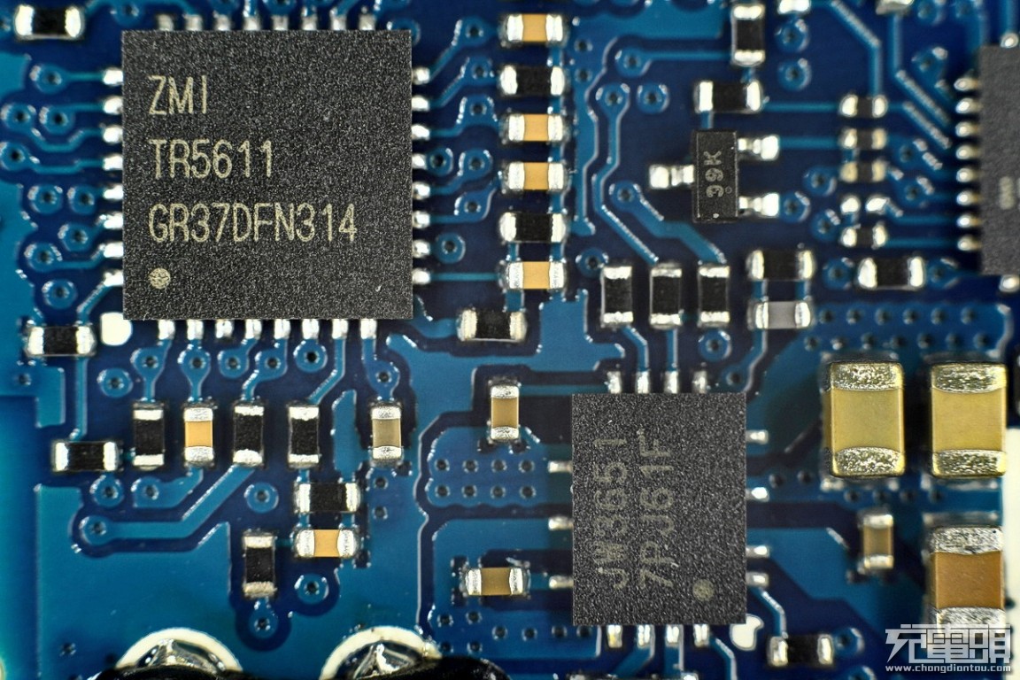
This is the TR5611 SCM.
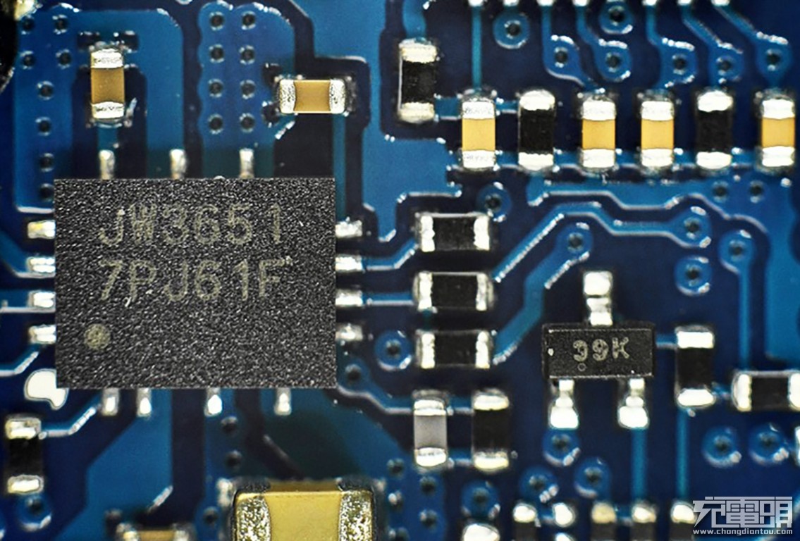
Joulwatt JW3651 converter is responsible for USB-A port fast charging output. It is an integrated four-switch buck-boost converter.
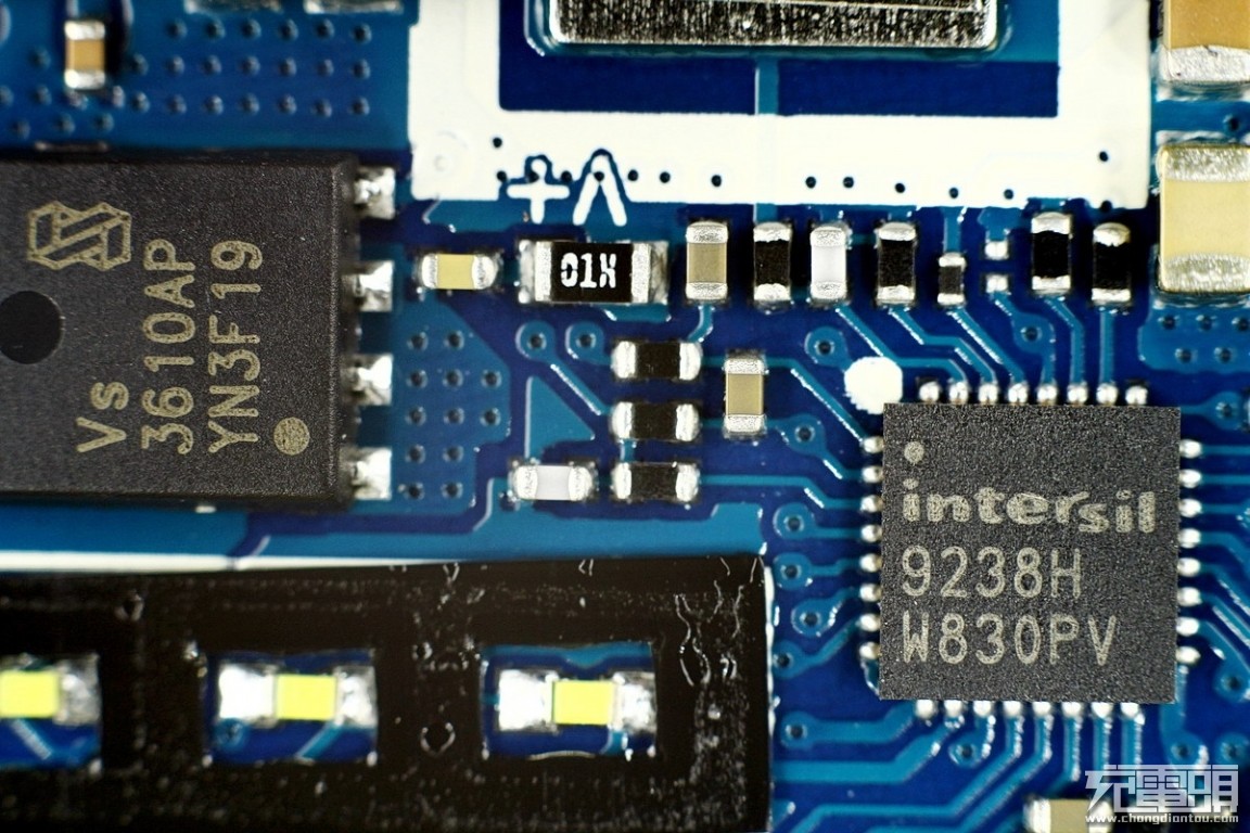
Intersil’s ISL9238 is a buck-boost Narrow Voltage DC(NVDC) charger.
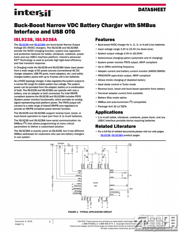
In Charging mode, the ISL9238 takes input power from a wide range of DC power sources (conventional AC/DC charger adapters, USB PD ports, travel adapters, etc.) and safely charge battery packs with up to 4-series cell Li-ion batteries. It provides the NVDC charging, system bus regulation and protection features for tablet, Ultrabook, notebook, power bank, and any USB-C interface platform.
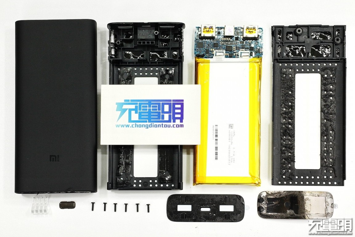
These are all the components of the Xiaomi Mi Power Bank 3 Pro.
Summary
We find that the Mi Power Bank 3 Pro version has made many breakthroughs on its circuit. For instance, it features Renesas ISL9238, Joulwatt JW3651 two buck-boost chips. Besides, the charger adopts TI BQ29200 battery voltage equalization chip. In general, the Xiaomi Mi Power Bank 3 Pro has excellent workmanship and adopts high-quality materials. One of the charger’s highlights is that its middle frame applies multiple roll cages.