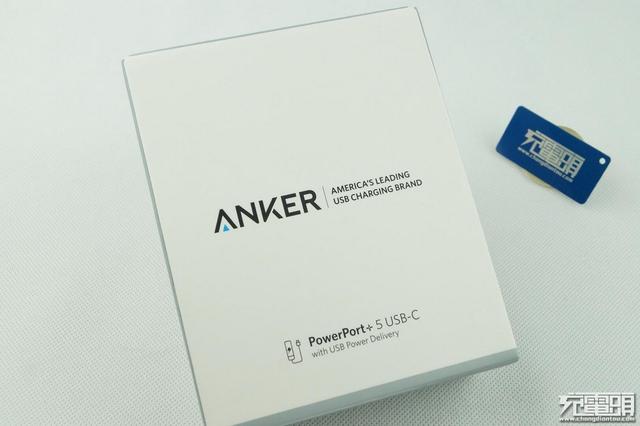
It boosts of Anker’s classic package.
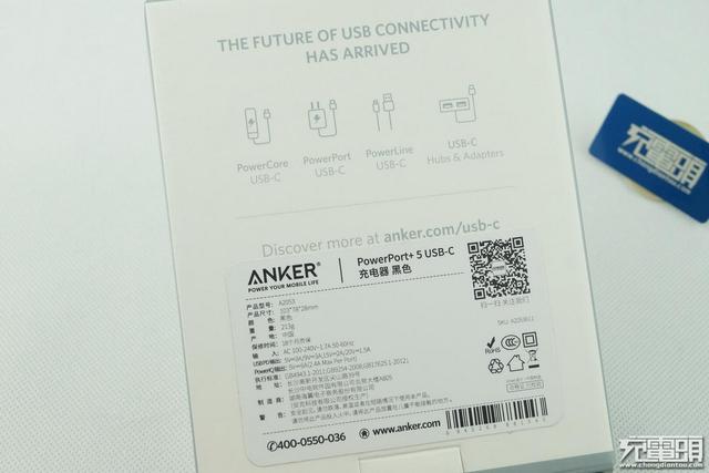
The power supply’s specification on the back of the box is elaborate.
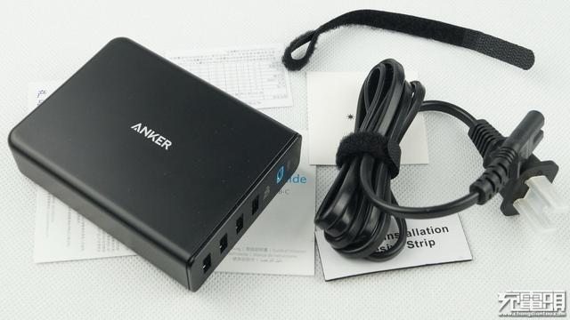
The power supply’s accessory is the power cord.

The power supply has brief design both on its front and back.
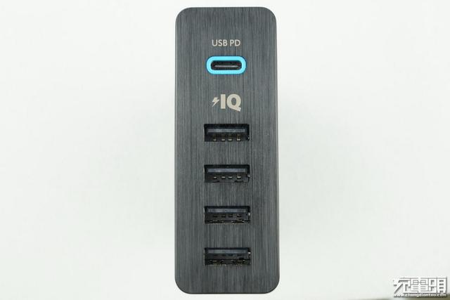
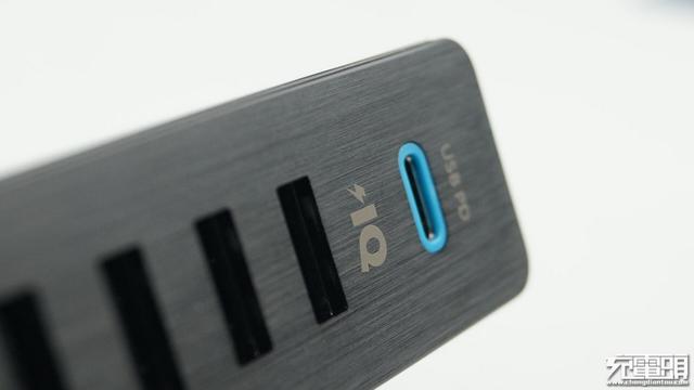
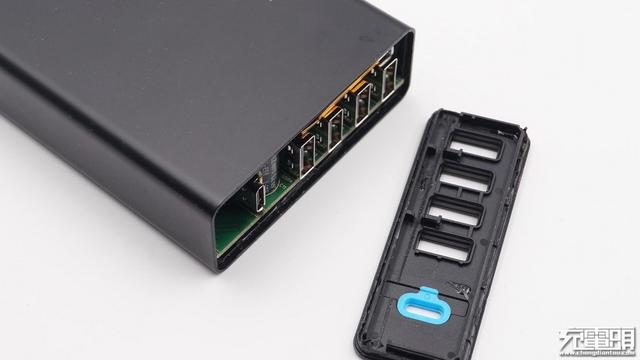
The black metal wire drawing panel brings good texture. The conspicuous blue PD output port is on the top. Below the PD output port lie four Power IQ USB output sockets.
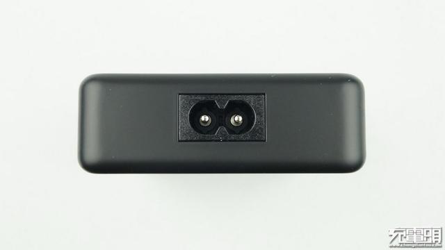
The AC input is universal.
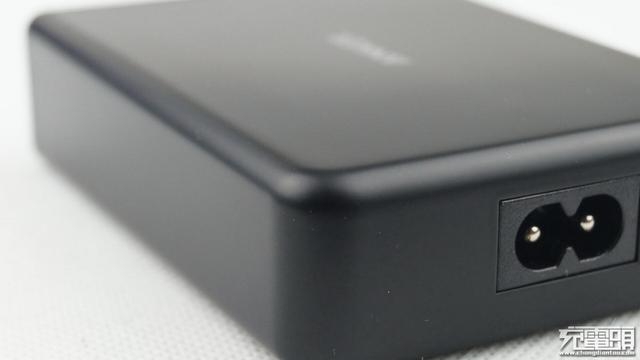
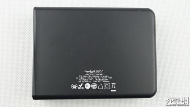
The power supply’s round angles bring good touch feeling.
The top cover adopts the ultrasonic welding technique.
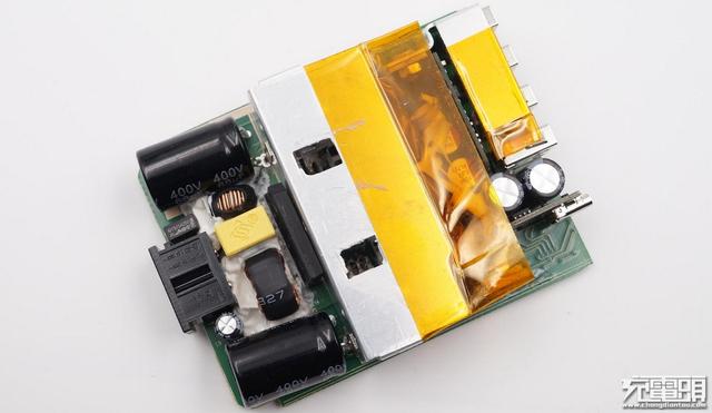
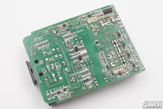
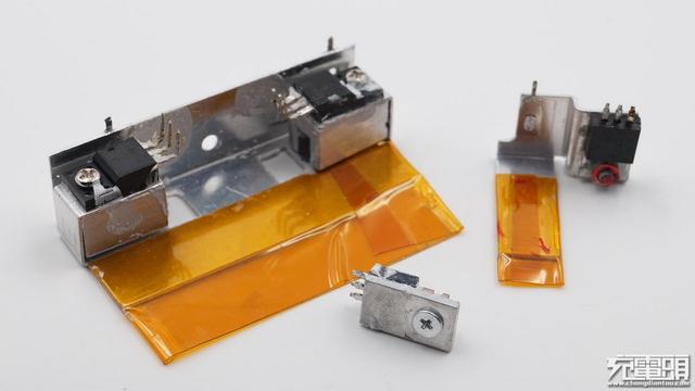
Two sides of the power supply circuit.
These are the AC input protection circuit and EIMI circuit.
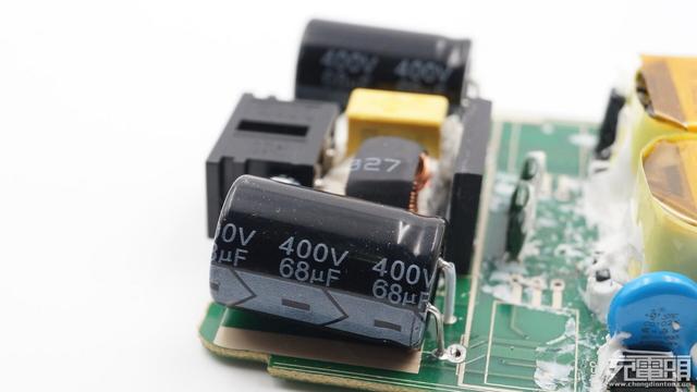
The two main capacitors have the same specification.
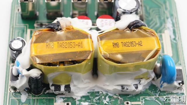
Two transformers
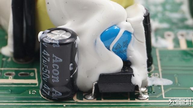

There are two blue anti-interference capacitors.
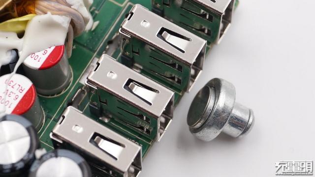
Four USB sockets
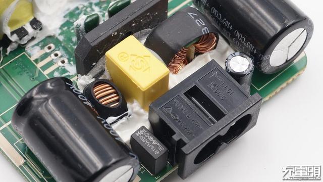
Remove the pipe with thermal foils. The biggest thermal foils are two PWM MOS.
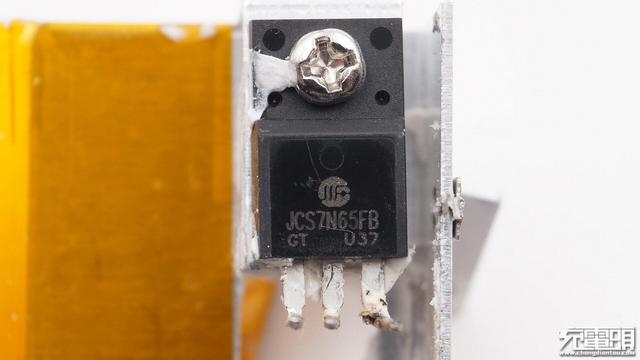
JCS7N65FB.
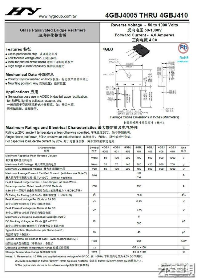
Two PWM MOS share the same bridge rectifier- HY GBJ410.
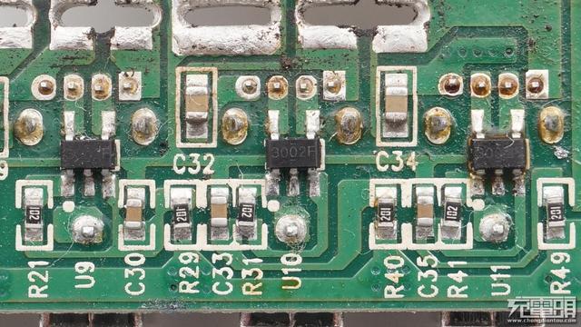
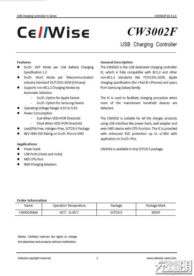
It is the USB intelligent sensor IC- cellwise-semi CW3002F.
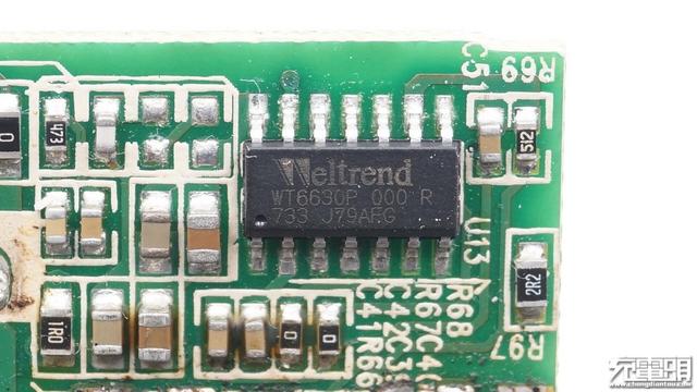
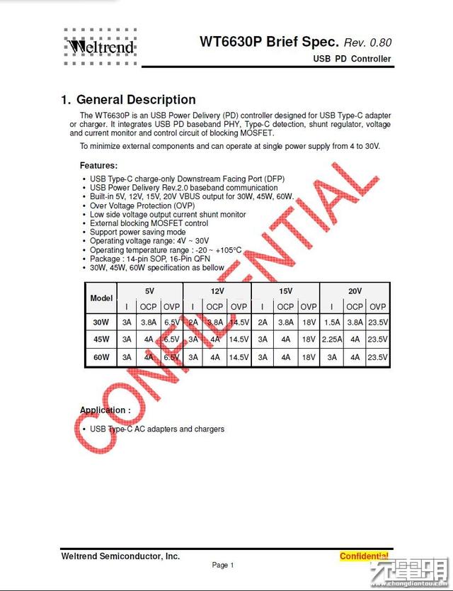
It is the PD output controller- Weltrend WT6630p.
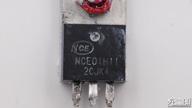
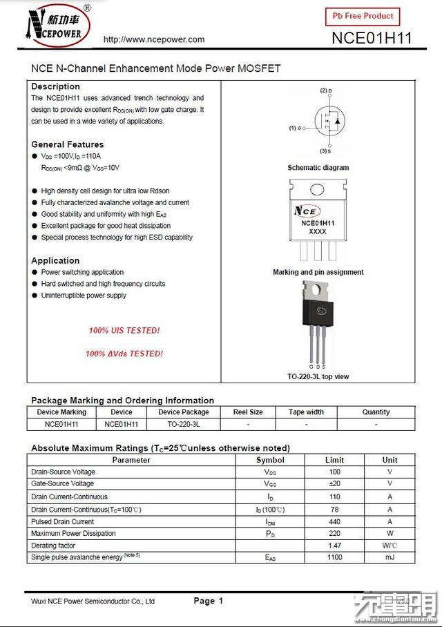
PD output synchronous rectifier MOS. NCE01H11.
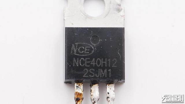
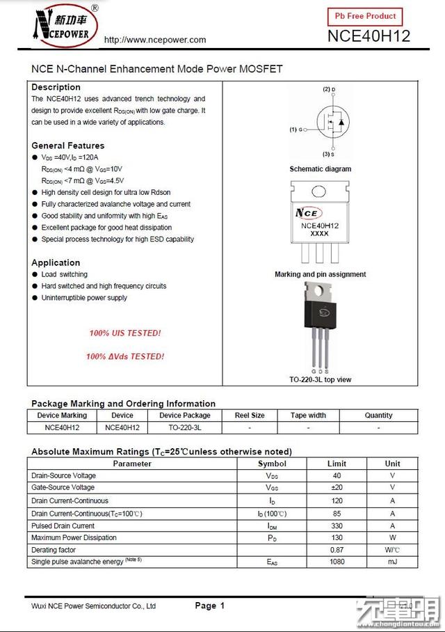
USB output synchronous rectifier MOS. NCE40A12.
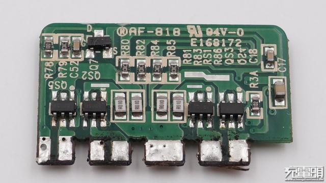
The USB output protects two sides of the daughterboard.
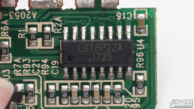
It is the single chip – LGT8P22A.
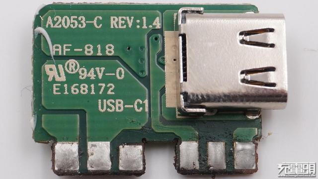
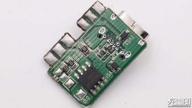
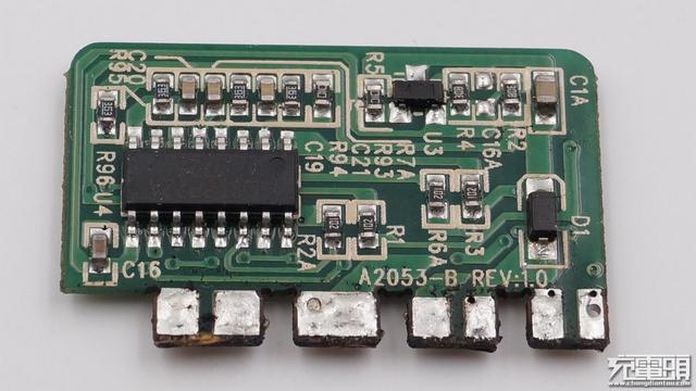
Two sides of the USB Type-C port’s daughterboard.
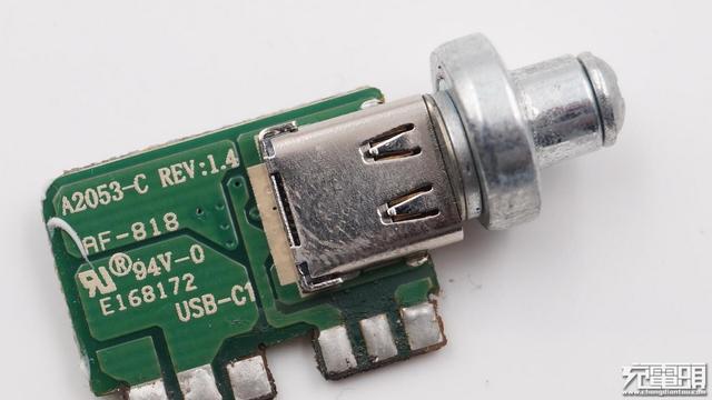
USB Type-C socket
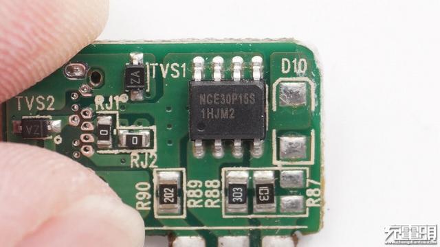
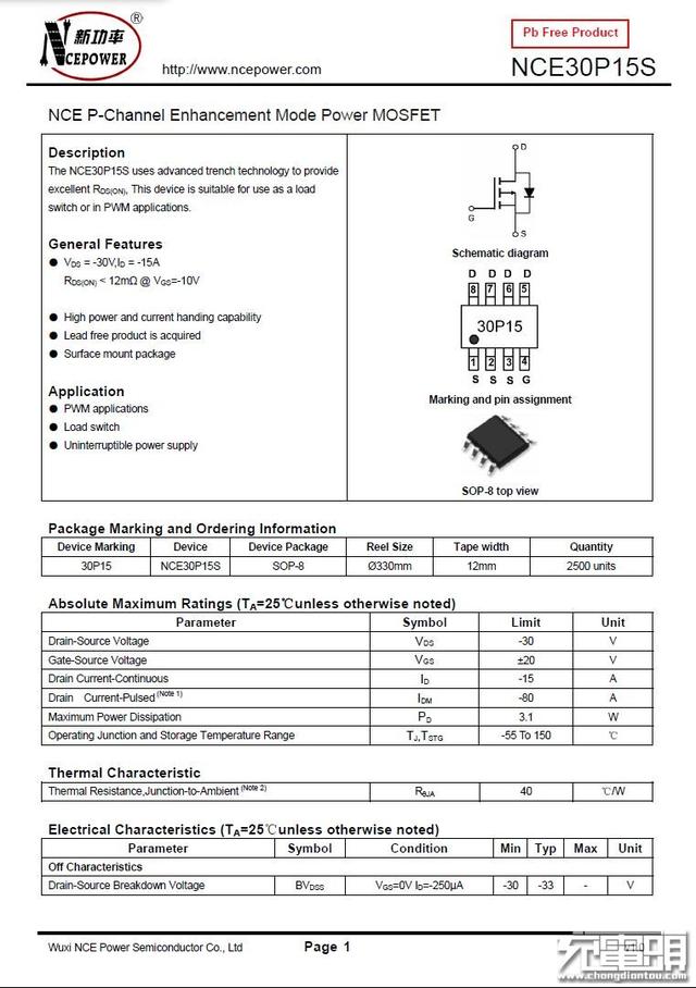
The USB Type-C output protects MOS. NCE30P15S.
After using the Power-Z to start the fast charge mode, we find that four USB ports only support Apple BC1.2.
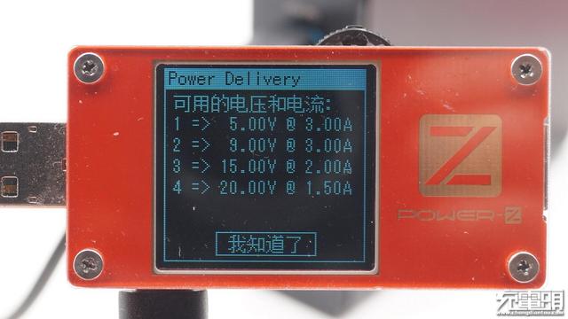
Use the Power-Z to start the USB Type-C port’s PD mode, and the results show the maximum currents that different voltage supports under the PD mode. The results keep the same with the specification on the package.
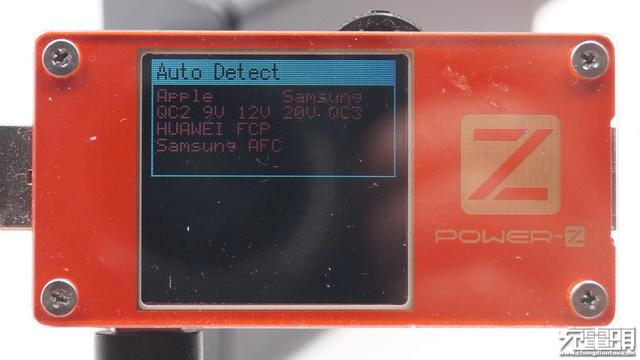
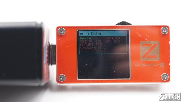
Use the Power-Z to start fast charge mode, and we find that the USB Type C port doesn’t support popular fast charge modes.