Last month, Huawei held a new product launch event in London to introduce the Huawei Mate 20 Pro. The Mate 20 Pro is powered by the world’s first 7nm mobile AI chip, the Kirin 980. This phone features an under-screen fingerprint reader. Today, we will take apart its internal structure and workmanship.
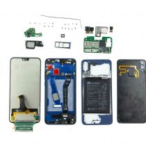
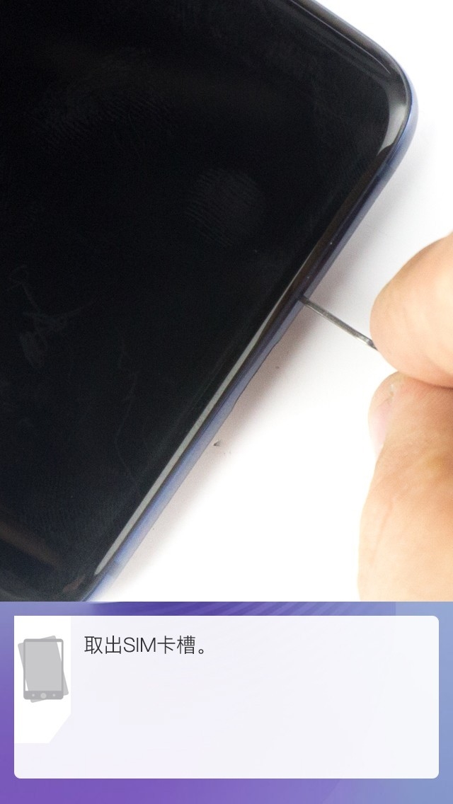
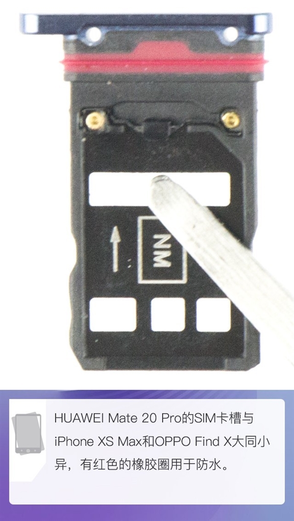
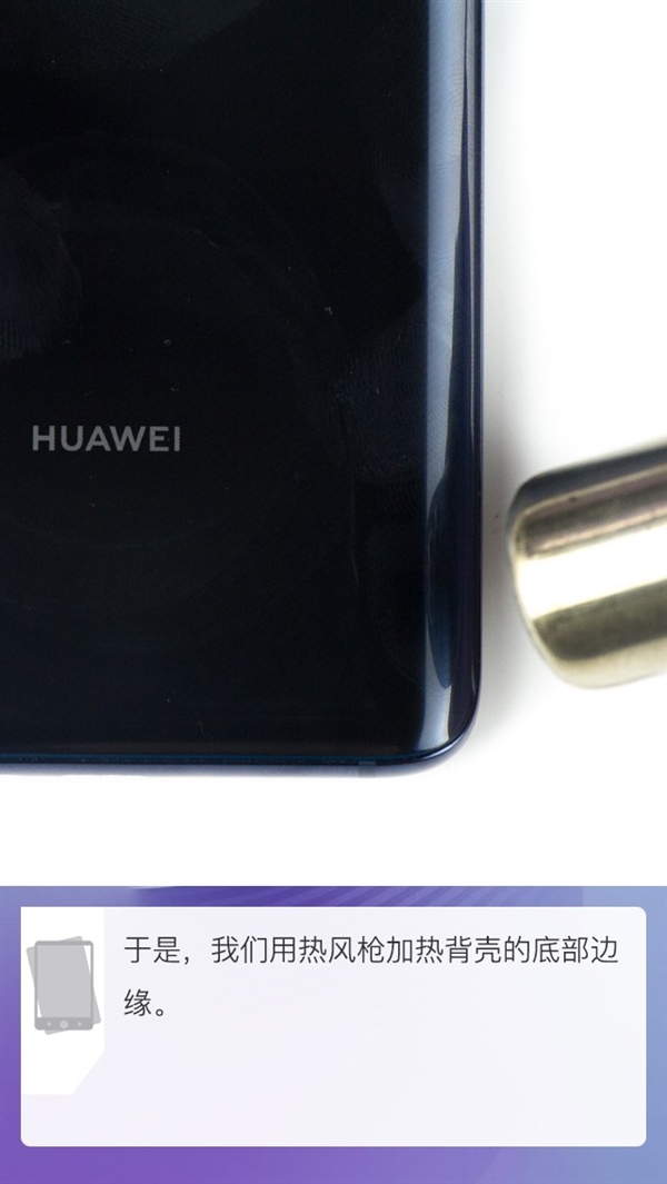
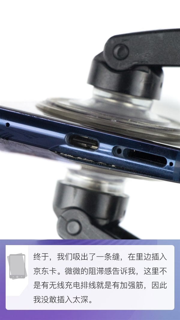
First, remove the SIM card tray. The red rubber on the tray prevents water and dust from entering the phone. We use a heat gun to heat the edge of the back cover. Then, we use a suction cup to separate the back cover from the phone body.
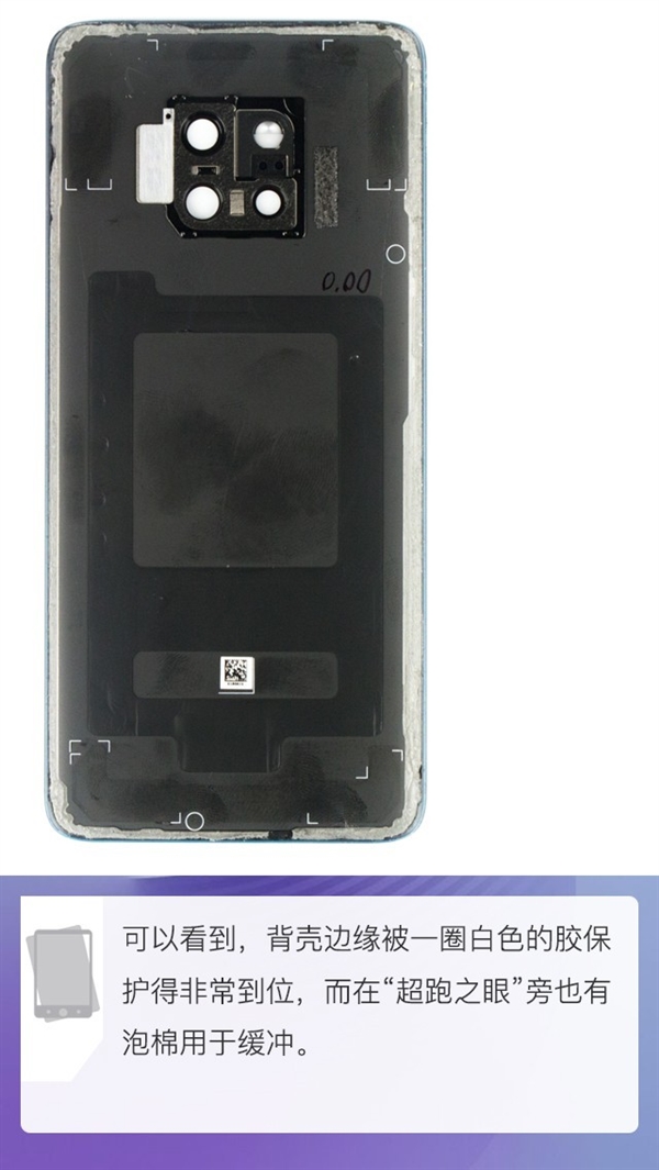
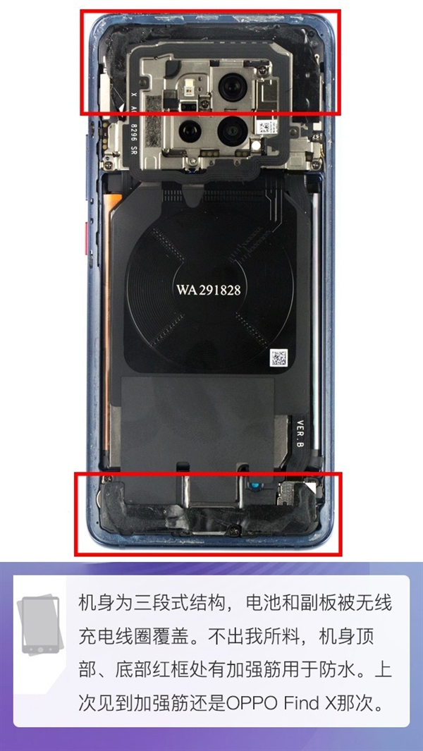
All four corners of the back cover are well protected by white glue. It can be seen that the phone adopts a classic three-section internal design: the battery and sub-board are covered by the wireless charging coil, while the top and bottom are lined with special waterproof materials.
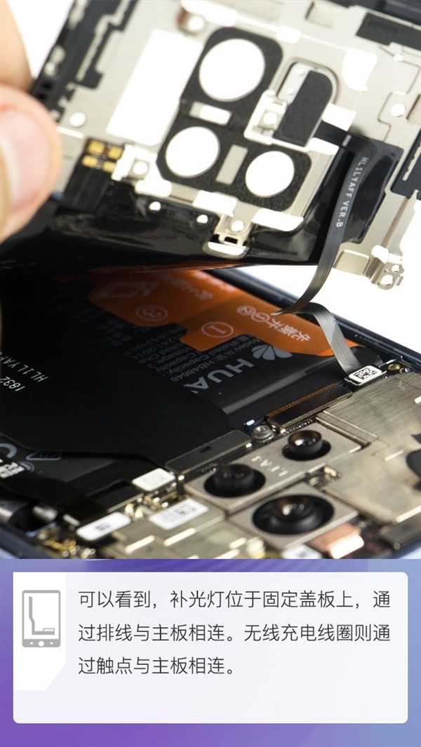
As shown in the image, the fill light is mounted on the plate. It connects to the main board via a cable, while the wireless charging coil is connected to the main board via metal contacts.
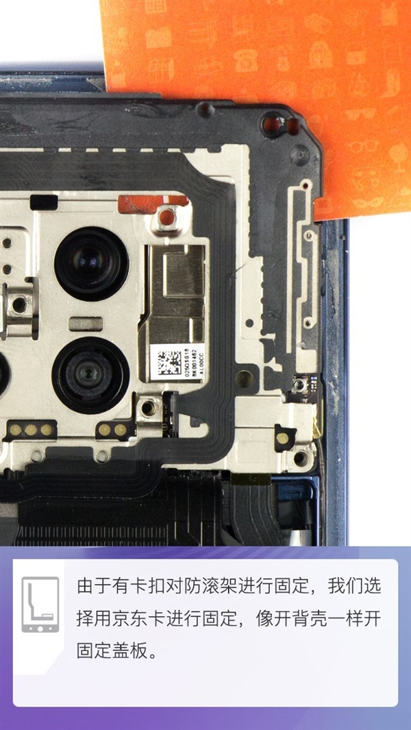
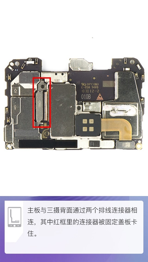
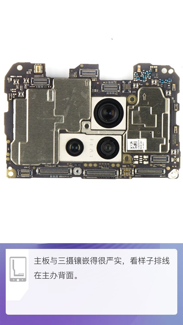
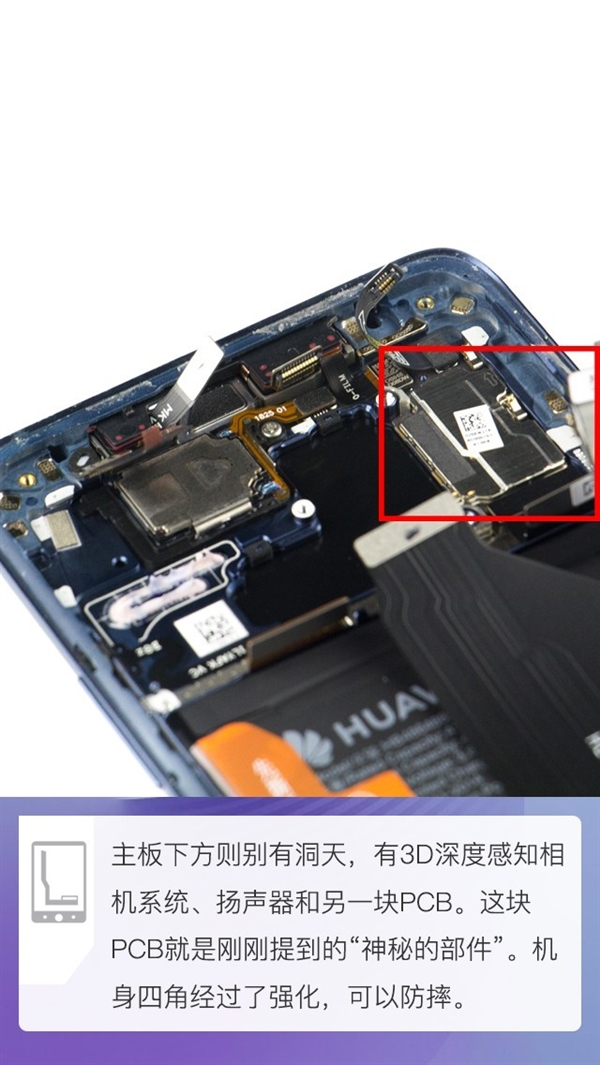
The three cameras are connected to the motherboard via two cables. The connector marked with a red circle is secured with a metal plate. The 3D depth-sensing camera system, speaker, and board are placed below the motherboard.
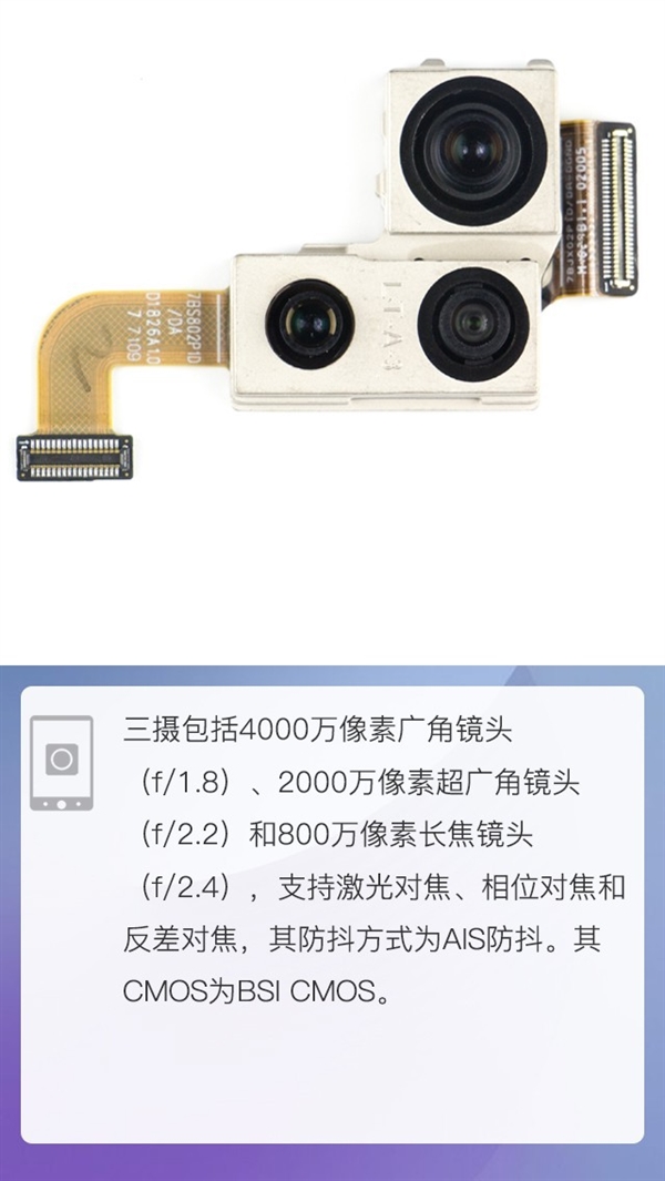
This phone features a Leica triple camera on the rear, including a 40MP wide-angle lens with an f/1.8 aperture, a 20MP ultra-wide-angle lens with an f/2.2 aperture, and an 8MP telephoto lens with an f/2.4 aperture. The Leica triple camera supports autofocus and Huawei AI Image Stabilization (AIS).
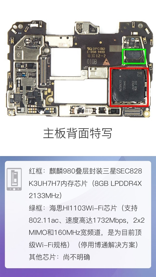
On the front of the motherboard, the part circled in red is the Kirin 980 chip and Samsung SEC828 K3UH7H7 memory chip (8GB LPDDR4X 2133MHz). The part circled in green is the Hisilion HI1103 Wi-Fi chip, which supports 802.11ac, 2×2 MIMO, and 160 MHz bandwidth. Its speed reaches up to 1732 Mbps. At present, this Wi-Fi chip reaches the top level.
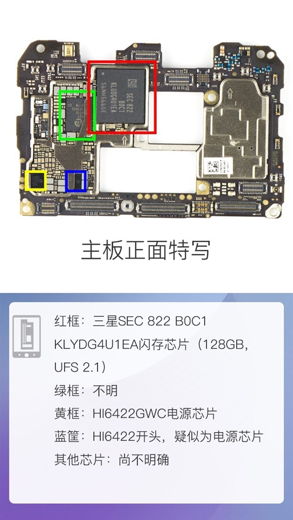
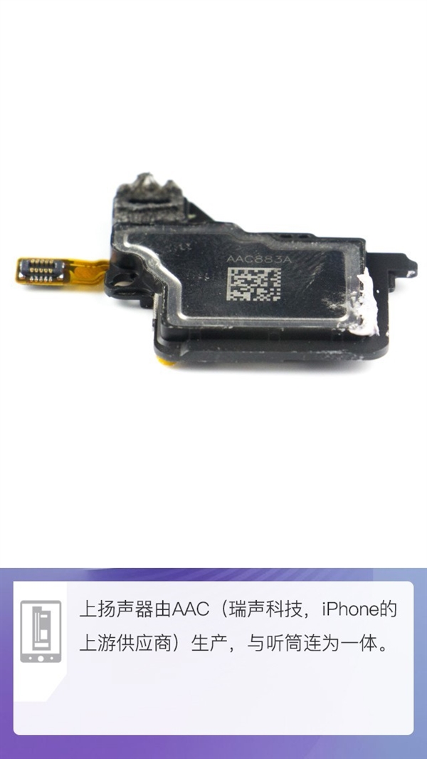
On the back of the motherboard, the part circled in red is the Samsung SEC 822 BOC1 KLYDG4U1EA flash chip (128GB, UFS 2.1). The part circled in yellow is the HI6422GWC power chip. The part circled in blue is the HI6422 chip, which we suppose is a power management chip. Its speaker is made by AAC.
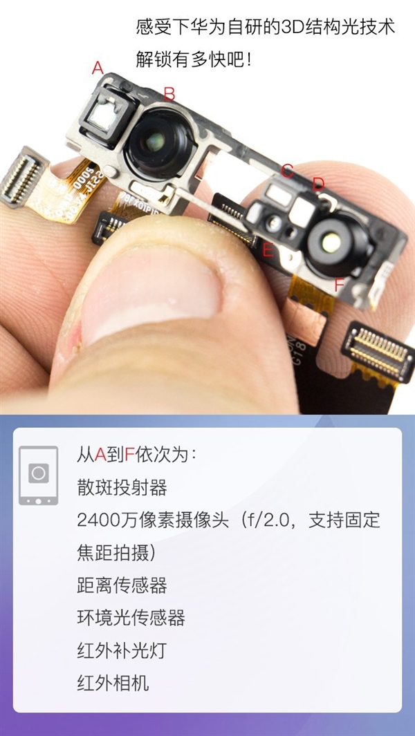
The components are: A: laser sensor; B: 24MP camera (f/2.0 aperture); C: proximity sensor; D: ambient light sensor; E: infrared flash; F: an infrared camera.
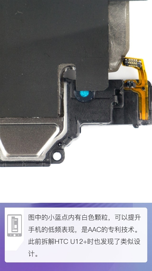
The white particles in the blue dot can enhance the phone’s low-frequency performance, which is ACC’s patented technology. The HTC U12 adopts a similar design.
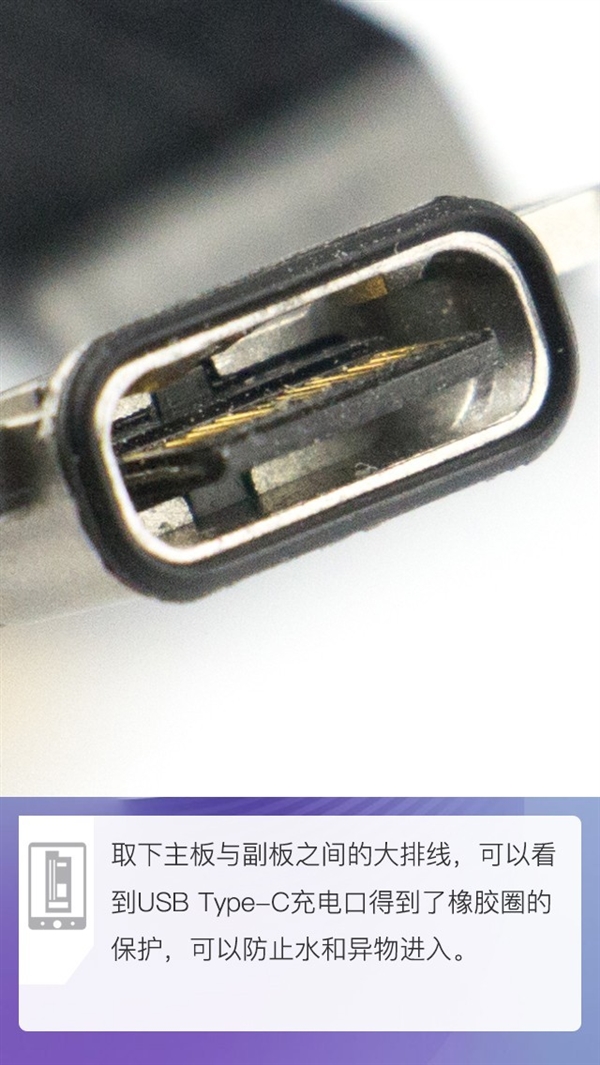
Disconnect the cable between the motherboard and the sub-board. The USB Type-C charging port is designed with a white rubber to prevent water and other materials from entering the phone.
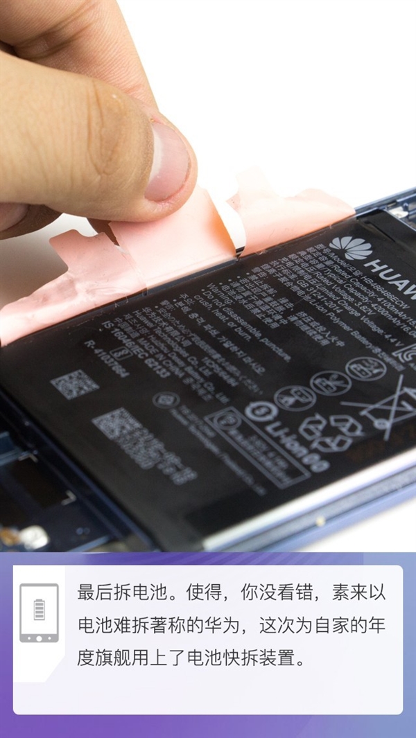
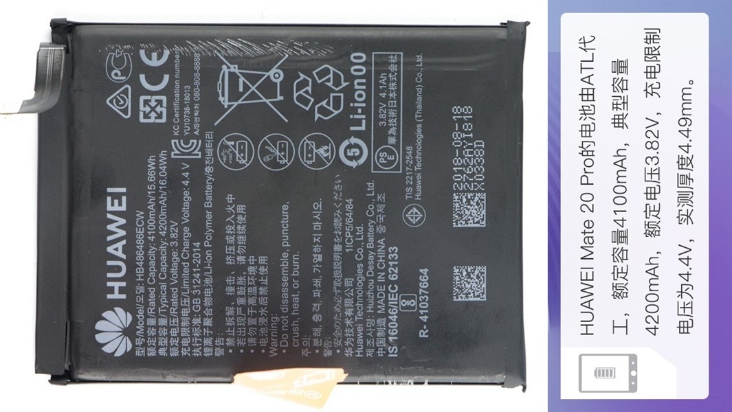
Now, we will take out its battery. This battery cell comes from ATL, and the battery is assembled by Huizhou Desay Battery Co., LTD. Its rated capacity is 4100 mAh, and its typical capacity is 4200 mAh; its rated voltage is 3.82V, and its limited charge voltage is 4.4V. Additionally, its thickness is 4.49mm.
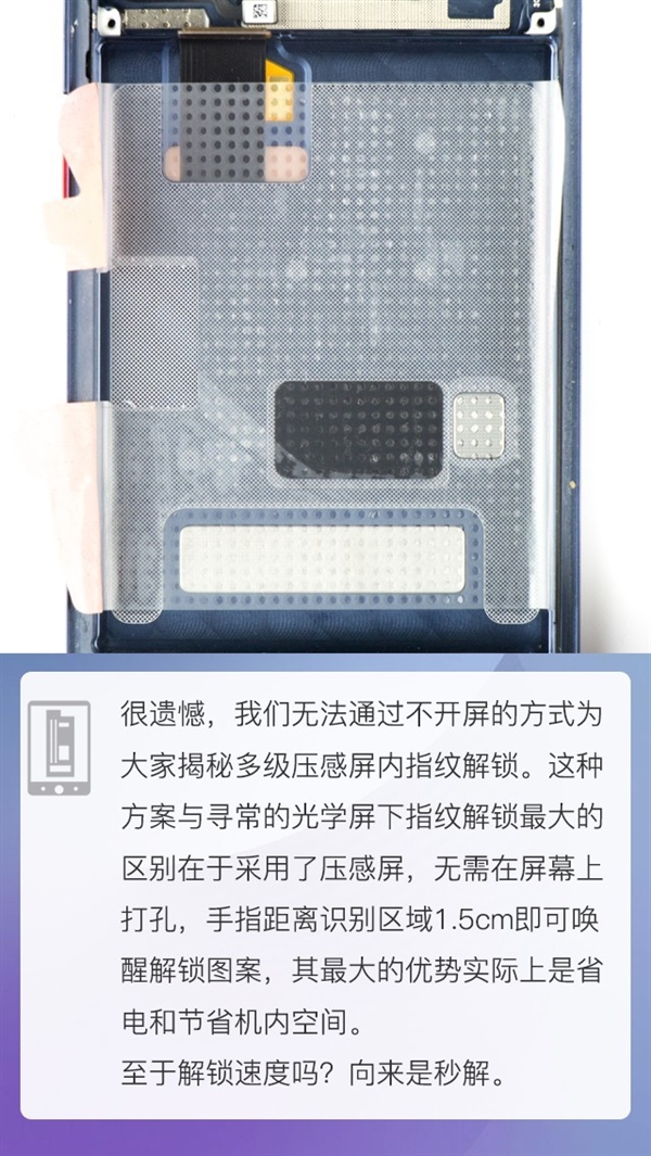
Unfortunately, I cannot show you the structure of its under-screen fingerprint reader, which uses dynamic pressure sensing technology. With this reader, users can unlock their phones securely and quickly.
Summary
The Huawei Mate 20 Pro has the best craftsmanship among all Huawei smartphones. It features flagship-level components and internal structures. Although the Mate 20 Pro has a complicated internal structure, its teardown process is simple.