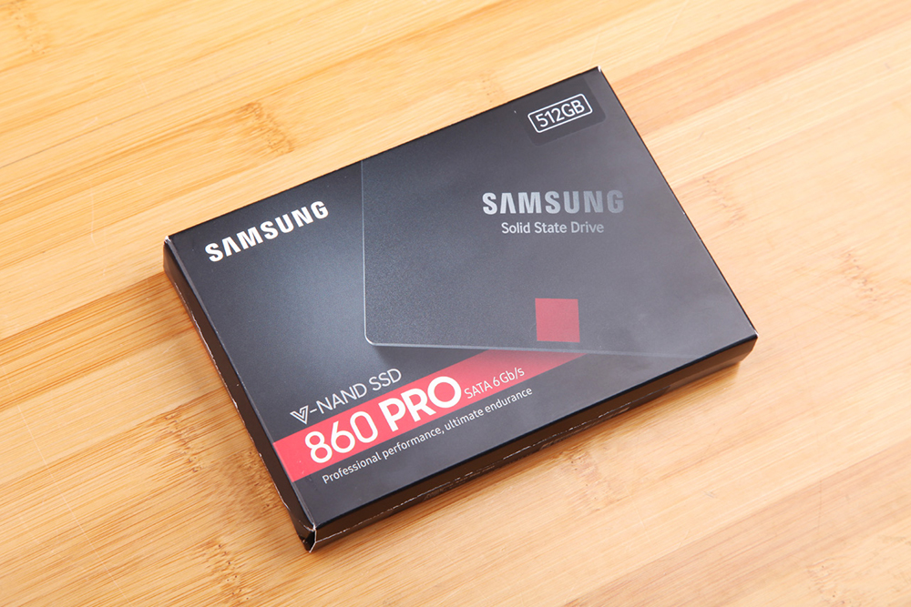
In early 2014, Samsung launched its first 3D NAND product for the consumer market, the 850 PRO series. About four years later, Samsung released the upgraded version of the 850 PRO, the 860 PRO series. Today, we will start to tear down the Samsung 860 PRO 512GB SSD.
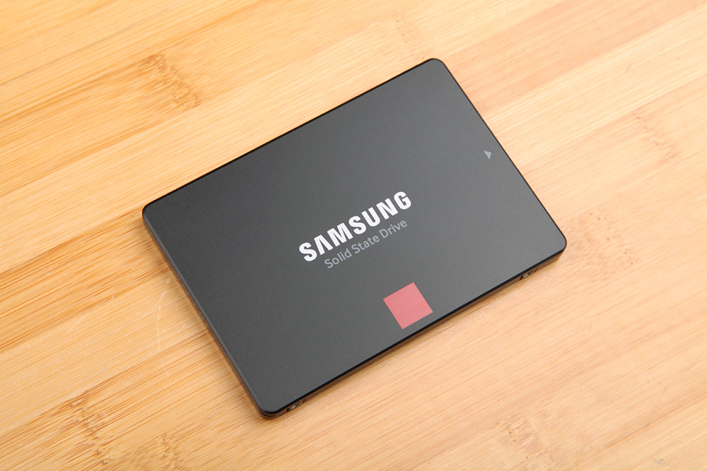
The Samsung 860 PRO is a 2.5-inch SSD. On the front of the drive, we can see the words ‘Samsung’ and ‘Solid State Drive’, but there is no product model number. A red box is located below the text. The arrow on the right indicates the port direction.
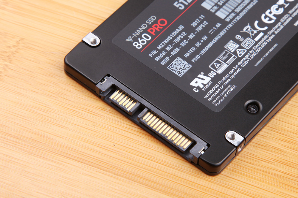
The back of the SSD contains more information, including the model number, capacity, production date, operating voltage, operating current, and so on. The 860 PRO that we will disassemble was manufactured in November 2017.
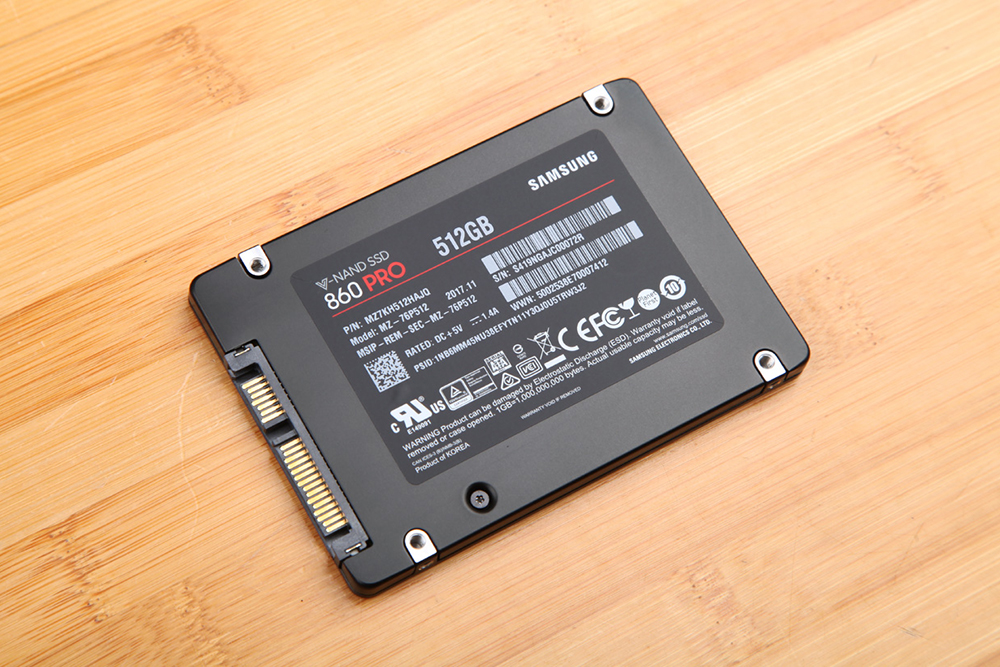
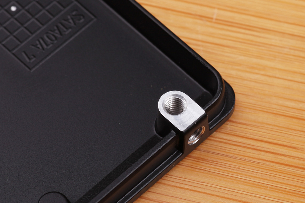
In general, the screws on the back of an SSD cannot be removed. However, the screw holes on the back of the Samsung 860 PRO are connected to the screw holes on the side, and all surfaces are polished.
The 7-pin connector on the left is a SATA 3.0 connector with a theoretical bandwidth of 6Gb/s. The 15-pin connector on the right is the power supply connector.
The sequential read and write speeds of the Samsung 860 PRO can reach up to 560MB/s and 530MB/s, respectively, while the random read and write speeds can reach up to 100K IOPS and 90K IOPS. This speed is not particularly impressive among SATA SSDs.
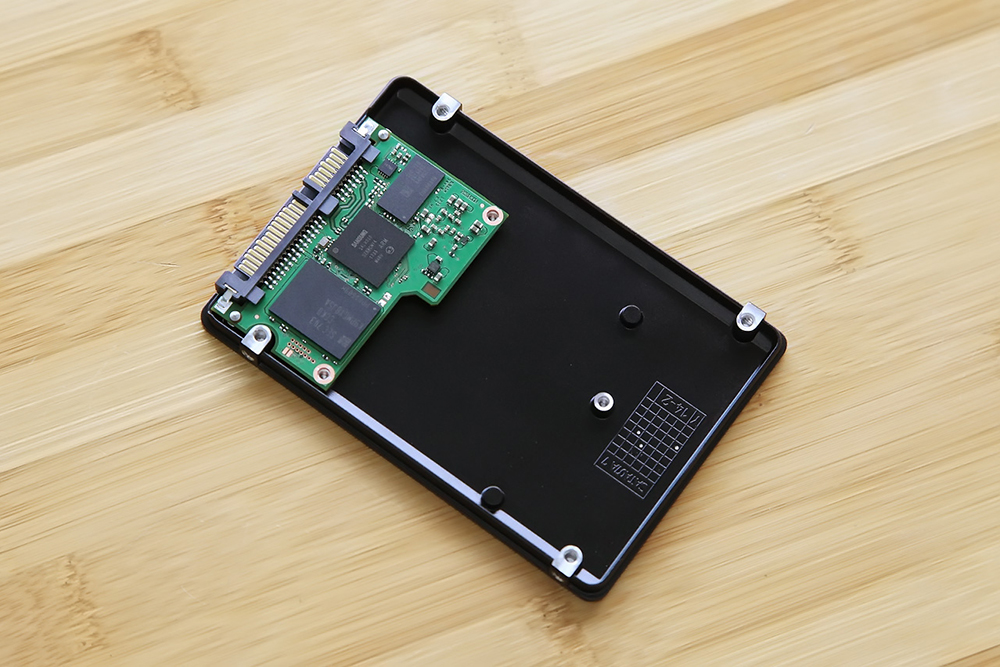
Remove the screws on the back of the SSD. This SSD uses pentagon screws, which are not very common. After removing the back cover, we found that the PCB of the 860 PRO is quite compact, only about one-third the size of the SSD.
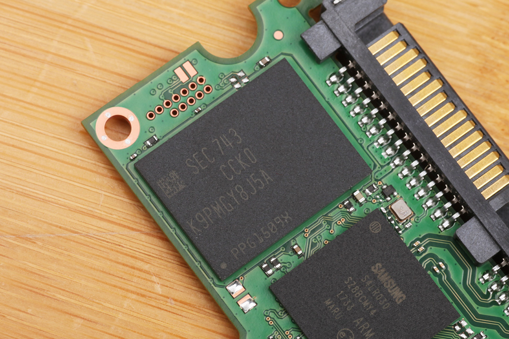
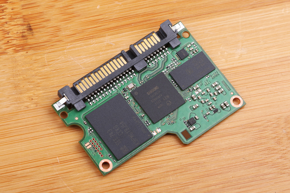
The front side of the PCB has a main control chip, a cache chip, a flash memory chip, and many capacitors.
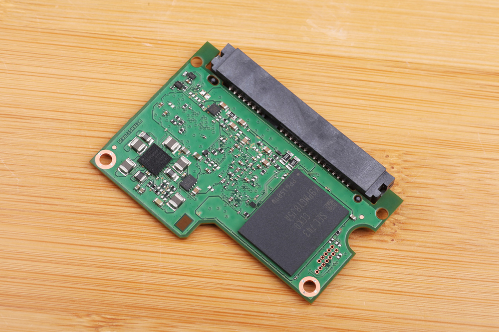
There is only one flash memory chip on the back of the PCB, and together with the one on the front, the two chips make up a total of 512GB of storage.
The main control chip uses Samsung’s MJX controller. Currently, specific information about the MJX controller (including core model, manufacturing process, etc.) is unknown. The only known information is that it supports LPDDR4 memory chips.
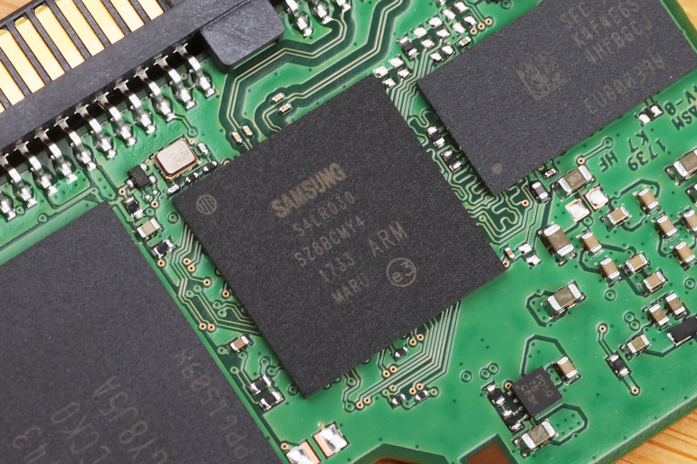
Close-up of the 512MB LPDDR4 cache chip
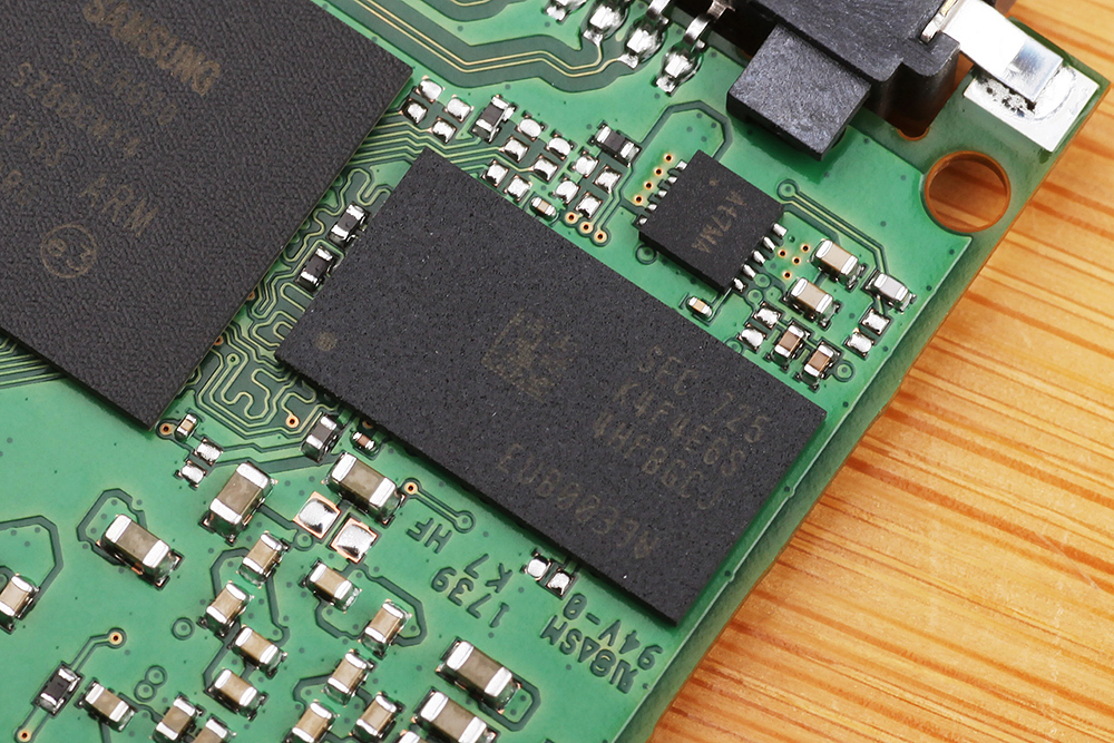
The flash memory chips are Samsung 3D MLC V-NAND, which is Samsung’s fourth-generation 3D NAND, with a single chip capacity of 256GB and a write life of 600TBW.